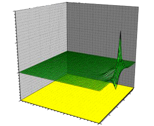
Excitation of short electric monopulse in nitride films with negative differential conductivity
DOI:
https://doi.org/10.3103/S0735272719060025Keywords:
nitride film, negative differential conductivity, space-charge wave, electric monopulseAbstract
The excitation of short electric monopulses of space charge waves with wide frequency spectrum of terahertz range in nitride films has been theoretically investigated. The excitation of these pulses with duration ≤5 ps and high peak values of electric fields is possible in n-GaN or n-InN films of submicron thickness in the presence of negative differential conductivity. The simulation of nonlinear dynamics of pulses was performed with due regard for the nonlocal dependence of the drift electron velocity on the average electron energy. Optimal values of the applied constant electric fields and equilibrium electron concentration for excitation of monopulses are specified. The monopulse dynamics is weakly dependent on the film width and also on the value and waveform of input excitation pulses. Short electric monopulses differ from domains of strong electric field in Gunn diodes built on bulk crystals with negative differential conductivity.References
- LEE, Yun-Shik. Principles of Terahertz Science and Technology. N.Y.: Springer, 2009. DOI: http://doi.org/10.1007/978-0-387-09540-0.
- PERENZONI, M.; PAUL, D.J. (eds.). Physics and Applications of Terahertz Radiation. N.Y.: Springer, 2014. DOI: http://doi.org/10.1007/978-94-007-3837-9.
- SONG, Ho-Jin; NAGATSUMA, Tadao, (eds.). Handbook of Terahertz Technologies: Devices and Applications. Boca Raton: CRC Press, 2015. URI: https://www.crcpress.com/Handbook-of-Terahertz-Technologies-Devices-and-Applications/Song-Nagatsuma/p/book/9789814613088.
- CARPINTERO, G.; GARCIA MUNOZ, L.E.; HARTNAGEL, H.L.; PREU, S.; RÄISÄNEN, A.V. (eds.). Semiconductor Terahertz Technology: Devices and Systems at Room Temperature Operation. N.Y.: John Wiley & Sons, 2015. DOI: http://doi.org/10.1002/9781118920411.
- NAKASHA, Y. “Foreword,” IEICE Trans. Electronics, v.E98.C, n.12, 2015. DOI: https://doi.org/10.1587/transele.E98.C.1058.
- VAKS, V.L.; BIRYUKOV, V.V.; KISILENKO, K.I.; PANIN, A.N.; PRIPOLZIN, S.I.; RAEVSKIY, A.S.; SCHERBAKOV, V.V. “Wireless communication systems of terahertz frequency range,” Zhurnal Radioelektroniki, n.12, p.1, 2018. DOI: http://doi.org/10.30898/1684-1719.2018.12.4.
- LUKIN, K.A.; MAKSYMOV, P.P. “Terahertz self-induced oscillations in the injection p–n junction with fixed reverse bias,” Radioelectron. Commun. Syst., v.53, n.8, p.405, 2010. DOI: https://doi.org/10.3103/S0735272710080029.
- PEARTON, S.J.; ZOLPER, J.C.; SHUL, R.J.; REN, F. “GaN: processing, defects, and devices,” J. Appl. Phys., v.86, n.1, p.1, 1999. DOI: https://doi.org/10.1063/1.371145.
- JAIN, S.C.; WILLANDER, M.; NARAYAN, J.; VAN OVERSTRAETEN, R. “III-nitrides: Growth, characterization, and properties,” J. Appl. Phys., v.87, n.3, p.965, 2000. DOI: https://doi.org/10.1063/1.371971.
- GRUZHINSKIS, V.; SHIKTOROV, P.; STARIKOV, E.; ZHAO, J.H. “Comparative study of 200-300 GHz microwave power generation in GaN TEDs by the Monte Carlo technique,” Semicond. Sci. Technol., v.16, n.8, p.798, 2001. DOI: https://doi.org/10.1088/0268-1242/16/9/311.
- LÜ, J.T.; CAO, J.C. “Terahertz generation and chaotic dynamics in GaN NDR diode,” Semicond. Sci. Technol., v.19, n.4, p.451, 2004. DOI: https://doi.org/10.1088/0268-1242/19/3/028.
- TIMOFEYEV, V.I.; SEMENOVSKAYA, E.V.; FALIEIEVA, O.M. “Electrothermal analysis of GaN power submicron field-effect heterotransistors,” Radioelectron. Commun. Syst., v.59, n.2, p.66, 2016. DOI: https://doi.org/10.3103/S0735272716020035.
- SHEREMET, V.N. “Formation peculiarities and properties of ohmic contacts to n-GaN(AlN) and artificial diamond,” Radioelectron. Commun. Syst., v.56, n.10, p.493, 2013. DOI: https://doi.org/10.3103/S073527271310004X.
- KOKOLOV, A.A.; BABAK, L.I. “Methodology of built and verification of non-linear EEHEMT model for GaN HEMT transistor,” Radioelectron. Commun. Syst., v.58, n.10, p.435, 2015. DOI: https://doi.org/10.3103/S0735272715100015.
- LEVINSHTEIN, M.; RUMYANTSEV, S.; SHUR, M. “Properties of advanced semiconductor materials: GaN, AlN, InN,” N.Y.: Wiley, 2001. URI: http://www.ioffe.ru/SVA/NSM/Semicond/GaN/.
- GRIMALSKY, V.; KOSHEVAYA, S.; MOROZ, I.; GARCIA-B., A. “Influence of nonlocality on amplification of space charge waves in n-GaN films,” Proc. of Int. Symp. on Phys. and Engineering of Microwaves, Millimeter and Submillimeter Waves, 21-26 June 2010, Kharkov, Ukraine. IEEE, 2010, p.1-4. DOI: https://doi.org/10.1109/msmw.2010.5546135.
- GRIMALSKY, V.; KOSHEVAYA, S.; TECPOYOTL-T., M.; DIAZ-A., F. “Influence of nonlocality on amplification of space charge waves in n-GaN films,” J. Electromagn. Analysis Appl., v.3, n.2, p.33, 2011. DOI: https://doi.org/10.4236/jemaa.2011.32006.
- FOLTIDES, E.J.; GRIMALSKY, V.; KOSHEVAYA, S.; ESCOBEDO-ALATORRE, J. “Amplification of space charge waves in n-InN films of THz range,” Proc. of IEEE MTT-S Latin America Microwave Conf., LAMC-2016, 12-14 Dec. 2016, Puerto Vallarta, Mexico. IEEE, 2016, p.1-3. DOI: https://doi.org/10.1109/lamc.2016.7851269.
- HADI, W.A.; GURAM, P.K.; SHUR, M.S.; O’LEARY, S.K. “Steady-state and transient electron transport within wurtzite and zinc-blende indium nitride,” J. Appl. Phys., v.113, n.11, paper 113709, 2013. DOI: https://doi.org/10.1063/1.4795146.
- SIDDIQUA, P.; HADI, W.A.; SALHOTRA, A.K.; SHUR, M.S.; O’LEARY, S.K. “Electron transport and electron energy distributions within the wurtzite and zinc-blende phases of indium nitride: Response to the application of a constant and uniform electric field,” J. Appl. Phys., v.117, n.12, Paper 125705, 2015. DOI: https://doi.org/10.1063/1.4915329.
- SZE, S.M.; NG, Kwok N. Physics of Semiconductor Devices. Hobokem NJ: Wiley-Interscience, 2007. DOI: http://doi.org/10.1002/0470068329.
- GARCIA-B., A.; GRIMALSKY, V.; GUTIERREZ-D., E.; KOSHEVAYA, S. “Dispersion relation for two-valley quasi-hydrodynamic models in SCWs propagation in n-GaAs thin films,” Proc. of 25th Int. Conf. on Microelectronics, 14-17 May 2006, Belgrade, Serbia. IEEE, 2006, p.507-510. DOI: https://doi.org/10.1109/icmel.2006.1651013.
- TOMIZAWA, K. Numerical Simulation of Submicron Semiconductor Devices. Boston: Artech House Pub., 1993.
- PRESS, W.H.; TEUKOLSKY, S.A.; VETTERLING, W.T.; FLANNERY, B.P. Numerical Recipes in Fortran. Cambridge: CUP, 1997.
- GRIMALSKY, V.; KOSHEVAYA, S.; TECPOYOTL-T., M.; ESCOBEDO-A., J. “Nonlinear interaction of terahertz and optical waves in nitride films,” Int. J. Terahertz Sci. Technol., v.6, n.3, p.165, 2013. DOI: http://doi.org/10.11906/TST.165-176.2013.09.10.

Downloads
Published
2019-06-27
Issue
Section
Research Articles

