Differential amplifier for biomedical signal acquisition applications based on stacked transistors
DOI:
https://doi.org/10.3103/S0735272724020043Keywords:
ECG, electrocardiogram, signal conditioning, high CMRR, PSRR, Input noiseAbstract
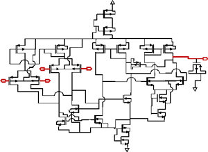
This study presents a two-stage differential amplifier circuit that has been improved for use in a realistic biomedical signal conditioning system. CMOS technology serves as the foundation for the circuit. A MOS-based low-pass filter using stacked transistors creates a low-power differential amplifier with low noise and high common-mode rejection ratio (CMRR) for portable electrocardiogram (ECG) signal conditioning. Stack transistors with MOS connected at the output terminal are used to improve the design for electrocardiogram (ECG) signal conditioning and other types of signal conditioning for biomedical devices. Standard 45nm CMOS process technology was used in the construction of the amplifier that is being discussed. The amplifier runs at a supply voltage of 0.85 V. The simulation findings are produced using the Cadence Analogue Virtuoso Spectre Simulator to generate the simulation. The differential amplifier described demonstrates a CMRR = 140 dB at frequency of 80 Hz, a power supply rejection ratio (PSRR) of 68 decibels, and a power dissipation of 1.3 mW. These characteristics conform to the simulation results. While the slew rate is 11 V/s, the input-referred noise is 2.62 mV/Hz1/2. Compared to the conventional differential amplifier, the performance characteristics generated by this approach are better and more efficient than those created by the standard circuit. The proposed design improves the noise performance of the differential amplifier developed in the past, which enhances noise performance.
References
- S. Lerstaveesin, M. Gupta, D. Kang, B.-S. Song, “A 48–860 MHz CMOS low-IF direct-conversion DTV tuner,” IEEE J. Solid-State Circuits, vol. 43, no. 9, pp. 2013–2024, 2008, doi: https://doi.org/10.1109/JSSC.2008.2001900.
- N. Meena, A. M. Joshi, “New power gated SRAM cell in 90nm CMOS technology with low leakage current and high data stability for sleep mode,” in 2014 IEEE International Conference on Computational Intelligence and Computing Research, 2014, pp. 1–5, doi: https://doi.org/10.1109/ICCIC.2014.7238333.
- C.-H. Li, C.-W. Lai, C.-N. Kuo, “A 147 GHz fully differential D-band amplifier design in 65 nm CMOS,” in 2013 Asia-Pacific Microwave Conference Proceedings (APMC), 2013, pp. 691–693, doi: https://doi.org/10.1109/APMC.2013.6694937.
- M. El-Nozahi, A. A. Helmy, E. Sanchez-Sinencio, K. Entesari, “An inductor-less noise-cancelling broadband low noise amplifier with composite transistor pair in 90 nm CMOS technology,” IEEE J. Solid-State Circuits, vol. 46, no. 5, pp. 1111–1122, 2011, doi: https://doi.org/10.1109/JSSC.2011.2118310.
- P. P. Babu, K. Sindhuja, T. D. Sri Sai Lakshmi, G. Sowmya, D. Akshitha, “Design and evaluation of two stage op-amp for biomedical applications using 90nm CMOS technology,” in 2024 7th International Conference on Devices, Circuits and Systems (ICDCS), 2024, pp. 174–178, doi: https://doi.org/10.1109/ICDCS59278.2024.10560856.
- K.-H. Chen, S.-I. Liu, “Inductorless wideband CMOS low-noise amplifiers using noise-canceling technique,” IEEE Trans. Circuits Syst. I Regul. Pap., vol. 59, no. 2, pp. 305–314, 2012, doi: https://doi.org/10.1109/TCSI.2011.2162461.
- J. W. Park, B. Razavi, “A harmonic-rejecting CMOS LNA for broadband radios,” IEEE J. Solid-State Circuits, vol. 48, no. 4, pp. 1072–1084, 2013, doi: https://doi.org/10.1109/JSSC.2013.2237651.
- P. Jain, A. M. Joshi, “Low leakage and high CMRR CMOS differential amplifier for biomedical application,” Analog Integr. Circuits Signal Process., vol. 93, no. 1, pp. 71–85, 2017, doi: https://doi.org/10.1007/s10470-017-1027-y.
- N. Van Thienen, P. Reynaert, “A 160-GHz three-stage fully-differential amplifier in 40-nm CMOS,” in 2014 21st IEEE International Conference on Electronics, Circuits and Systems (ICECS), 2014, pp. 144–147, doi: https://doi.org/10.1109/ICECS.2014.7049942.
- H.-C. Lee, C.-S. Wang, C.-K. Wang, “A 0.2–2.6 GHz wideband noise-reduction Gm-boosted LNA,” IEEE Microw. Wirel. Components Lett., vol. 22, no. 5, pp. 269–271, 2012, doi: https://doi.org/10.1109/LMWC.2012.2191275.
- P. Jain, A. Joshi, “Full-wave bridge rectifier with CMOS pass transistors configuration,” J. Circuits, Syst. Comput., vol. 27, no. 06, p. 1850092, 2018, doi: https://doi.org/10.1142/S0218126618500925.
- S. Jin, B. Park, K. Moon, M. Kwon, B. Kim, “Linearization of CMOS cascode power amplifiers through adaptive bias control,” IEEE Trans. Microw. Theory Tech., vol. 61, no. 12, pp. 4534–4543, 2013, doi: https://doi.org/10.1109/TMTT.2013.2288206.
- K. Sharma, S. Singh, A. Sachdeva, “A low-power low-noise amplifier with high CMRR for wearable healthcare applications,” AEU - Int. J. Electron. Commun., vol. 173, p. 154994, 2024, doi: https://doi.org/10.1016/j.aeue.2023.154994.
- S. Jin, M. Kwon, K. Moon, B. Park, B. Kim, “Control of IMD asymmetry of CMOS power amplifier for broadband operation using wideband signal,” IEEE Trans. Microw. Theory Tech., vol. 61, no. 10, pp. 3753–3762, 2013, doi: https://doi.org/10.1109/TMTT.2013.2280116.
- K. Choi et al., “A highly linear two-stage amplifier integrated circuit using InGaP/GaAs HBT,” IEEE J. Solid-State Circuits, vol. 45, no. 10, pp. 2038–2043, 2010, doi: https://doi.org/10.1109/JSSC.2010.2061612.
- R. A. Gayakwad, Op-Amps and Linear Integrated Circuits. New Delhi: Prentice-Hall, 2007.
- Q. Huang, M. Oberle, “A 0.5-mW passive telemetry IC for biomedical applications,” IEEE J. Solid-State Circuits, vol. 33, no. 7, pp. 937–946, 1998, doi: https://doi.org/10.1109/4.701225.
- Y. Hu, M. Sawan, “A fully integrated low-power BPSK demodulator for implantable medical devices,” IEEE Trans. Circuits Syst. I Regul. Pap., vol. 52, no. 12, pp. 2552–2562, 2005, doi: https://doi.org/10.1109/TCSI.2005.858163.
- J. Lee, G.-H. Lee, H. Kim, S. Cho, “An ultra-high input impedance analog front end using self-calibrated positive feedback,” IEEE J. Solid-State Circuits, vol. 53, no. 8, pp. 2252–2262, 2018, doi: https://doi.org/10.1109/JSSC.2018.2831231.
- Y. Zhao, Z. Shang, Y. Lian, “A 2.55 NEF 76 dB CMRR DC-coupled fully differential difference amplifier based analog front end for wearable biomedical sensors,” IEEE Trans. Biomed. Circuits Syst., vol. 13, no. 5, pp. 918–926, 2019, doi: https://doi.org/10.1109/TBCAS.2019.2924416.
- S. Masui, E. Ishii, T. Iwawaki, Y. Sugawara, K. Sawada, “A 13.56 MHz CMOS RF identification transponder integrated circuit with a dedicated CPU,” in 1999 IEEE International Solid-State Circuits Conference. Digest of Technical Papers. ISSCC. First Edition (Cat. No.99CH36278), 1999, pp. 162–163, doi: https://doi.org/10.1109/ISSCC.1999.759174.
- P. Jain, S. Akashe, “Analysis of ATPMOS configurations-based 4×1 multiplexer with estimation of power and delay,” Int. J. Electron., vol. 101, no. 7, pp. 1006–1018, 2014, doi: https://doi.org/10.1080/00207217.2013.805391.
- P. Jain, S. Akashe, “An innovative design: MOS based full-wave centre-tapped rectifier,” Wirel. Pers. Commun., vol. 90, no. 4, pp. 1673–1693, 2016, doi: https://doi.org/10.1007/s11277-016-3417-3.
- M. M. Ahmadi, G. A. Jullien, “A wireless-implantable microsystem for continuous blood glucose monitoring,” IEEE Trans. Biomed. Circuits Syst., vol. 3, no. 3, pp. 169–180, 2009, doi: https://doi.org/10.1109/TBCAS.2009.2016844.
- S. Ethier, M. Sawan, “Exponential current pulse generation for efficient very high-impedance multisite stimulation,” IEEE Trans. Biomed. Circuits Syst., vol. 5, no. 1, pp. 30–38, 2011, doi: https://doi.org/10.1109/TBCAS.2010.2073707.
- P. Jain, S. Akashe, “Power delay optimization of nanoscale 4×1 multiplexer using CMOS based voltage doubler circuit,” Radioelectron. Commun. Syst., vol. 59, no. 11, pp. 477–488, 2016, doi: https://doi.org/10.3103/S0735272716110017.
- P. Jain, A. M. Joshi, “Analyzing the impact of augmented transistor NMOS configuration on parameters of 4x1 multiplexer,” Radioelectron. Commun. Syst., vol. 61, no. 3, pp. 121–127, 2018, doi: https://doi.org/10.3103/S0735272718030044.
- P. S. Kumar, V. Ch, S. Thouti, G. P. Kumar, N. Rajeswaran, “High gain more stable self biased two stage differential amplifier for bio-signal processing,” in 2023 9th International Conference on Advanced Computing and Communication Systems (ICACCS), 2023, pp. 1859–1863, doi: https://doi.org/10.1109/ICACCS57279.2023.10112830.
- P. Rajeswari, V. Manikandan, “Buck converter current measurement using differential amplifier,” Intell. Autom. Soft Comput., vol. 35, no. 2, pp. 1387–1402, 2023, doi: https://doi.org/10.32604/iasc.2023.025866.
- N. Prokopenko, V. Chumakov, M. Sergeenko, “Differential amplifiers and DAC discharging current switches with differentiating transient correction circuits,” in 2023 Wave Electronics and its Application in Information and Telecommunication Systems (WECONF), 2023, pp. 1–4, doi: https://doi.org/10.1109/WECONF57201.2023.10148051.