Influence of surface morphology of silicon nanowire array on their humidity-sensitive characteristics
DOI:
https://doi.org/10.3103/S0735272723110018Keywords:
silicon nanowires, nanofibers, surface roughness, humidity sensitivity, humidity sensor, atomic force microscopy, metal-stimulated chemical etchingAbstract
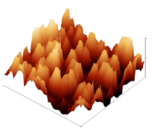
The paper investigates the influence of the surface morphology of an array of silicon nanowires (SNW) on their humidity-sensitive characteristics. In this work, diode-type moisture sensors based on silicon nanowires were synthesized. SNWs were synthesized by the method of metal-stimulated chemical etching, and a p–n junction was formed in the SNW array by diffusion. The surface morphology was studied by the method of atomic force microscopy. The electrical and moisture-sensitive characteristics of the humidity sensors were measured. The influence of the root mean square value (RMS) of surface roughness and the volume porosity of material on the performance of the devices was determined. In particular, it has been shown that an increase in the surface roughness of the silicon nanowire array leads to a significant increase in the response (by up to 72.5 times), as well as a decrease in the response time and the recovery time of humidity sensors amounting to 20 and 36 s, respectively. On the other hand, the reduction of the roughness RMS leads to an improvement in reversibility (up to 11.3%), short-term stability (up to 1.61%), and repeatability of the sensor signal (up to 0.45%). The importance of taking into account the relationship between the surface morphology of the array of nanowires and their humidity-sensitive characteristics for the development of high-performance nanowire-based sensors has been demonstrated.
References
- N. Mohseni Kiasari, S. Soltanian, B. Gholamkhass, P. Servati, “Room temperature ultra-sensitive resistive humidity sensor based on single zinc oxide nanowire,” Sensors Actuators A Phys., vol. 182, pp. 101–105, 2012, doi: https://doi.org/10.1016/j.sna.2012.05.041.
- V. R. Karrevula, A. K. Prasad, V. Mishra, S. Tripurasundari, “Effect of pre-adsorbed moisture and humidity on I–V characteristics of Si PIN diode,” Nucl. Instruments Methods Phys. Res. Sect. A Accel. Spectrometers, Detect. Assoc. Equip., vol. 1047, p. 167832, 2023, doi: https://doi.org/10.1016/j.nima.2022.167832.
- V. A. Lapshuda, Y. O. Linevych, M. H. Dusheiko, V. M. Koval, V. A. Barbash, “Capacitive humidity sensors based on nanocellulose for biodegradable electronics,” Microsystems, Electron. Acoust., vol. 27, no. 1, pp. 255990-1-255990–8, 2022, doi: https://doi.org/10.20535/2523-4455.mea.255990.
- H. M. J. Al-Ta’ii, Y. M. Amin, V. Periasamy, “Humidity influenced capacitance and resistance of an Al/DNA/Al Schottky diode irradiated by alpha particles,” Sci. Reports, vol. 6, no. 1, p. 25519, 2016, doi: https://doi.org/10.1038/srep25519.
- A. K. Kalkan, H. Li, C. J. O’Brien, S. J. Fonash, “A rapid-response, high-sensitivity nanophase humidity sensor for respiratory monitoring,” IEEE Electron Device Lett., vol. 25, no. 8, pp. 526–528, 2004, doi: https://doi.org/10.1109/LED.2004.832657.
- H.-J. Chen, Q.-Z. Xue, M. Ma, X.-Y. Zhou, “Capacitive humidity sensor based on amorphous carbon film/n-Si heterojunctions,” Sensors Actuators B Chem., vol. 150, no. 1, pp. 487–489, 2010, doi: https://doi.org/10.1016/j.snb.2010.07.038.
- J. Qin et al., “Carbon nanodot-based humidity sensor for self-powered respiratory monitoring,” Nano Energy, vol. 101, p. 107549, 2022, doi: https://doi.org/10.1016/j.nanoen.2022.107549.
- Z. Li et al., “Highly sensitive and stable humidity nanosensors based on LiCl doped TiO2 electrospun nanofibers,” J. Am. Chem. Soc., vol. 130, no. 15, pp. 5036–5037, 2008, doi: https://doi.org/10.1021/ja800176s.
- V. Lapshuda, V. Koval, V. Barbash, M. Dusheiko, O. Yashchenko, S. Malyuta, “Flexible humidity sensors based on nanocellulose,” in 2022 IEEE 41st International Conference on Electronics and Nanotechnology (ELNANO), 2022, pp. 208–212, doi: https://doi.org/10.1109/ELNANO54667.2022.9927092.
- Y. O. Linevych, V. M. Koval, “Sensors based on nanoscale silicon 1D structures for industrial, environmental and medical monitoring,” Microsystems, Electron. Acoust., vol. 27, no. 2, pp. 264376-1-264376–28, 2022, doi: https://doi.org/10.20535/2523-4455.mea.264376.
- M. Zeraati, T.-C. Chen, M. Ebri, N. P. S. Chauhan, G. Sargazi, “Length prediction of silicon nanowires (SiNWs) prepared by the MACE method using the ANN-COA-PSO algorithm for high supercapacitor applications,” J. Phys. Chem. Solids, vol. 156, p. 110146, 2021, doi: https://doi.org/10.1016/j.jpcs.2021.110146.
- Y. Xi et al., “A facile synthesis of silicon nanowires/micropillars structure using lithography and metal-assisted chemical etching method,” J. Solid State Chem., vol. 258, pp. 181–190, 2018, doi: https://doi.org/10.1016/j.jssc.2017.07.034.
- N. Ahmed, P. B. Bhargav, A. Rayerfrancis, B. Chandra, P. Ramasamy, “Study the effect of plasma power density and gold catalyst thickness on silicon nanowires growth by plasma enhanced chemical vapour deposition,” Mater. Lett., vol. 219, pp. 127–130, 2018, doi: https://doi.org/10.1016/j.matlet.2018.02.086.
- B. R. Deepu, S. M. Anil, P. Savitha, Y. B. Basavaraju, “Advanced VLS growth of gold encrusted silicon nanowires mediated by porous aluminium oxide template,” Vacuum, vol. 185, p. 109991, 2021, doi: https://doi.org/10.1016/j.vacuum.2020.109991.
- M. K. Sahoo, S. P. Muduli, P. Kale, “Tailoring electrical characteristics of Si-nanowires and etched Si by MACE temperature variation,” J. Mater. Sci. Mater. Electron., vol. 34, no. 16, p. 1275, 2023, doi: https://doi.org/10.1007/s10854-023-10709-y.
- A. A. Leonardi, M. J. Lo Faro, A. Irrera, “Silicon nanowires synthesis by metal-assisted chemical etching: A review,” Nanomaterials, vol. 11, no. 2, p. 383, 2021, doi: https://doi.org/10.3390/nano11020383.
- M. K. Sahoo, P. G. Kale, “Micro-Raman study of growth parameter restraint for silicon nanowire synthesis using MACE,” Superlattices Microstruct., vol. 135, p. 106289, 2019, doi: https://doi.org/10.1016/j.spmi.2019.106289.
- C. Chiappini, X. Liu, J. R. Fakhoury, M. Ferrari, “Biodegradable porous silicon barcode nanowires with defined geometry,” Adv. Funct. Mater., vol. 20, no. 14, pp. 2231–2239, 2010, doi: https://doi.org/10.1002/adfm.201000360.
- Z. Huang, T. Shimizu, S. Senz, Z. Zhang, N. Geyer, U. Gösele, “Oxidation rate effect on the direction of metal-assisted chemical and electrochemical etching of silicon,” J. Phys. Chem. C, vol. 114, no. 24, pp. 10683–10690, 2010, doi: https://doi.org/10.1021/jp911121q.
- G. Zhang et al., “Nanowire-based sensor electronics for chemical and biological applications,” Analyst, vol. 146, no. 22, pp. 6684–6725, 2021, doi: https://doi.org/10.1039/D1AN01096D.
- H. Taghinejad, M. Taghinejad, M. Abdolahad, A. Saeidi, S. Mohajerzadeh, “Fabrication and modeling of high sensitivity humidity sensors based on doped silicon nanowires,” Sensors Actuators B Chem., vol. 176, pp. 413–419, 2013, doi: https://doi.org/10.1016/j.snb.2012.09.062.
- Y. Linevych, V. Koval, M. Dusheiko, Y. Yakymenko, M. Lakyda, V. Barbash, “Silicon diode structures based on nanowires for temperature sensing application,” in 2022 IEEE 41st International Conference on Electronics and Nanotechnology (ELNANO), 2022, pp. 190–195, doi: https://doi.org/10.1109/ELNANO54667.2022.9927122.
- V. M. Koval et al., “Application of nanostructured silver film in multilayer contact system of Ti/Mo/Ag silicon photoconverters,” Radioelectron. Commun. Syst., vol. 59, no. 2, pp. 53–59, 2016, doi: https://doi.org/10.3103/S0735272716020011.
- Y. Linevych, V. Koval, M. Dusheіko, M. Lakyda, “Humidity diode sensors based on 1D nanosized silicon structures,” Sci. Innov., vol. 20, no. 3, pp. 67–81, 2024, doi: https://doi.org/10.15407/scine20.03.067.
- Z. Chen, C. Lu, “Humidity sensors: A review of materials and mechanisms,” Sens. Lett., vol. 3, no. 4, pp. 274–295, 2005, doi: https://doi.org/10.1166/sl.2005.045.
- J. P. Lukaszewicz, “An application of carbon-type semiconductors for the construction of a humidity-sensitive diode,” Sensors Actuators B Chem., vol. 6, no. 1–3, pp. 61–65, 1992, doi: https://doi.org/10.1016/0925-4005(92)80031-R.