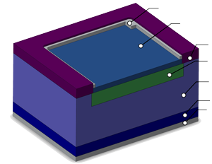
Temperature drift of silicon photodiode spectral sensitivity
DOI:
https://doi.org/10.3103/S073527272302005XKeywords:
A3B5 solid solutions, metalorganic chemical vapour deposition, MOCVD, emissivity- compensated pyrometry, silicon photodiode, temperature dependence of parametersAbstract
The spectral sensitivity change of a silicon photodiode with its temperature is analyzed in the article. This research area is relevant because silicon photodiodes are used as sensitive elements in temperature control systems of the vapour-phase epitaxy process. Technical characteristics of the obtained semiconductor devices are mostly determined by the quality of heterostructures used for their manufacture. The optical pyrometry method is used for the surface temperature precise control of the A3B5 solid solutions active layers during metalorganic chemical vapour deposition (MOCVD). Since the surface relief and parameters during deposition change significantly, classical pyrometry leads to significant measurement errors, so the pyrometry method with radiation compensation is used. This method combines the wafer surface radiation measurement and its reflectivity. This allows to determine the surface temperature true value, the layer thickness and the heat distribution uniformity on the wafer in real time.
However, for high precision, it is necessary to take into account the temperature coefficient of the silicon photodiode ampere-watt sensitivity change. The basics of MOCVD technology are discussed in this article. The features of the epitaxy process in the reactor with high-precision temperature control are highlighted.
The analytical and empirical study of change in silicon photodiode ampere-watt sensitivity and its effect on measurement accuracy are given. The research results improve the accuracy of real temperature measurement using pyrometric parameter control systems in MOCVD technology and help to understand and to take into account the influence of temperature factors on measurement accuracy to improve this technology.
References
- J. R. Creighton, W. G. Breiland, D. D. Koleske, G. Thaler, M. H. Crawford, “Emissivity-correcting mid-infrared pyrometry for group-III nitride MOCVD temperature measurement and control,” J. Cryst. Growth, vol. 310, no. 6, pp. 1062–1068, 2008, doi: https://doi.org/10.1016/j.jcrysgro.2007.12.063.
- S. I. Krukovskyi, V. Arikov, A. O. Voronko, V. S. Antonyuk, “Features of low-temperature GaAs formation for epitaxy device structures,” J. Nano- Electron. Phys., vol. 14, no. 2, pp. 02016-1-02016–5, 2022, doi: https://doi.org/10.21272/jnep.14(2).02016.
- D. F. Storm et al., “Dependence of growth temperature on the electrical properties and microstructure of MBE-grown AlN/GaN resonant tunneling diodes on sapphire,” J. Vac. Sci. Technol. B, Nanotechnol. Microelectron. Mater. Process. Meas. Phenom., vol. 38, no. 3, 2020, doi: https://doi.org/10.1116/6.0000052.
- H. Ghadi et al., “Influence of growth temperature on defect states throughout the bandgap of MOCVD-grown β -Ga2O3,” Appl. Phys. Lett., vol. 117, no. 17, 2020, doi: https://doi.org/10.1063/5.0025970.
- M. Belousov, B. Volf, J. C. Ramer, E. A. Armour, A. Gurary, “In situ metrology advances in MOCVD growth of GaN-based materials,” J. Cryst. Growth, vol. 272, no. 1–4, pp. 94–99, 2004, doi: https://doi.org/10.1016/j.jcrysgro.2004.08.080.
- A. Gurary, “Application of emissivity compensated pyrometry for temperature measurement and control during compound semiconductors manufacturing,” in AIP Conference Proceedings, 2003, vol. 684, pp. 843–848, doi: https://doi.org/10.1063/1.1627233.
- H. Photonics, “Silicon photodiode basics,” Si photodiodes, 2022. https://www.hamamatsu.com/content/dam/hamamatsu-photonics/sites/documents/99_SALES_LIBRARY/ssd/si_pd_kspd0001e.pdf.
- J. Hartmann, J. Fischer, U. Johannsen, L. Werner, “Analytical model for the temperature dependence of the spectral responsivity of silicon,” J. Opt. Soc. Am. B, vol. 18, no. 7, p. 942, 2001, doi: https://doi.org/10.1364/JOSAB.18.000942.
- H. A. Weakliem, D. Redfield, “Temperature dependence of the optical properties of silicon,” J. Appl. Phys., vol. 50, no. 3, pp. 1491–1493, 1979, doi: https://doi.org/10.1063/1.326135.
- P. Geng, W. Li, X. Zhang, X. Zhang, Y. Deng, H. Kou, “A novel theoretical model for the temperature dependence of band gap energy in semiconductors,” J. Phys. D Appl. Phys., vol. 50, no. 40, p. 40LT02, 2017, doi: https://doi.org/10.1088/1361-6463/aa85ad.
- C. Schinke et al., “Uncertainty analysis for the coefficient of band-to-band absorption of crystalline silicon,” AIP Adv., vol. 5, no. 6, 2015, doi: https://doi.org/10.1063/1.4923379.
- J. Heller, J. W. Bartha, C. C. Poon, A. C. Tam, “Temperature dependence of the reflectivity of silicon with surface oxide at wavelengths of 633 and 1047 nm,” Appl. Phys. Lett., vol. 75, no. 1, pp. 43–45, 1999, doi: https://doi.org/10.1063/1.124271.
- L. Werner, J. Fischer, U. Johannsen, J. Hartmann, “Accurate determination of the spectral responsivity of silicon trap detectors between 238 nm and 1015 nm using a laser-based cryogenic radiometer,” Metrologia, vol. 37, no. 4, pp. 279–284, 2000, doi: https://doi.org/10.1088/0026-1394/37/4/3.
- V. G. Verbitskiy, V. S. Antonyuk, A. O. Voronko, L. M. Korolevych, D. V. Verbitskiy, D. O. Novikov, “Matrix of photosensitive elements for determining the coordinates of the source of optical radiation,” J. Nano- Electron. Phys., vol. 13, no. 4, pp. 04029-1-04029–6, 2021, doi: https://doi.org/10.21272/jnep.13(4).04029.


