Output buffer for +3.3 V applications in a 180 nm +1.8 V CMOS technology
DOI:
https://doi.org/10.3103/S0735272717110061Keywords:
PCI-X, buffer, level converter, voltage swing, propagation delay, voltage drop, peripheral component interconnect extendedAbstract
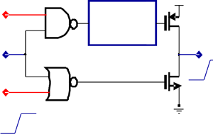
A new output buffer realized with low-voltage (+1.8 V) devices to drive high voltage signals for +3.3 V interface, such as peripheral component interconnect extended (PCI-X) applications in a 180 nm CMOS process is proposed in this paper. As PCI-X is a +3.3 V interface, the high voltage gate–oxide stress poses a serious problem to design PCI-X I/O circuits in a 180 nm CMOS process. The performance of the proposed output buffer is examined using Cadence software and the model parameters of a 180 nm CMOS process. The experimental results have hither to confirm that the proposed output buffer can be successfully operated at 100 MHz frequency without suffering high voltage gate–oxide overstress in the +3.3 V interface. A new level converter realized with +1.8 V devices that can convert 0/1 V voltage swing to 0/3.3 V voltage swing is also presented in this paper. The simulation results have confirmed that the proposed level converter can be operated accurately without any voltage drop. The topology, however, reports low sensitivity and has features suitable for VLSI implementation. The proposed circuits are suited for low power design without performance degradation.References
- LIN, Yingyan; ZOU, Xuecheng; ZHENG, Zhaoxiao; HUO, Wenjie; CHEN, Xiaofei; KANG, Wenjing. High-speed, low switching noise and load adaptive output buffer. Proc. of IEEE Int. Symp. on Integrated Circuits, ISIC, 14-16 Dec, 2009, Singapore. IEEE, 2009, p.280-282. URI: http://ieeexplore.ieee.org/document/5403888/.
- SCOTT, R.S.; DUMIN, N.A.; HUGHES, T.W.; DUMIN, D.J.; MOORE, B.T. Properties of high-voltage stress generated traps in thin silicon oxide. IEEE Trans. Electron Devices, v.43, n.7, p.1133-1143, 1996. DOI: https://doi.org/10.1109/16.502425.
- MAHENDRANATH, B.; SRINIVASULU, A. Analysis of two new voltage level converters with various load conditions. Int. J. Advances Telecommunications, Electrotechnics, Signals and Systems, v.2, n.3, p.92-98, 2013. URI: http://www.ijates.org/index.php/ijates/article/view/45.
- SRINIVASULU, A.; RAJESH, M. ULPD and CPTL pull-up stages for differential cascode voltage switch logic. J. Engineering, v.2013, Article ID 595296, 5 pages, 2013. DOI: http://dx.doi.org/10.1155/2013/595296.
- SUNDARI, A.B.T.; SRINIVASULU, Avireni. High speed level converters with short circuit current reduction. Int. J. Advances in Telecommunications, Electrotechnics, Signals and Systems, v.3, n.2, p.44-52, 2014. DOI: http://dx.doi.org/10.11601/ijates.v3i2.92.
- MAHENDRANATH, B.; SRINIVASULU, Avireni. Performance analysis of a new CMOS output buffer. Proc. of IEEE Int. Conf. on Circuits, Power and Computing Technologies, 20-21 Mar. 2013, Nagercoil, India. IEEE, 2013, p.752-755. DOI: https://doi.org/10.1109/ICCPCT.2013.6529041.
- PELGROM, M.J.M.; DIJKMANS, E.C. A 3/5 V compatible I/O buffer. IEEE J. Solid-State Circuits, v.30, n.7, p.823-825, 1995. DOI: https://doi.org/10.1109/4.391124.
- KER, M.-D.; TSAI, C.-S. Design of 2.5V/5V mixed-voltage CMOS I/O buffer with only thin oxide device and dynamic N-well bias circuit. Proc. of IEEE Int. Symp. on Circuits and Systems, 25-28 May 2003, Bangkok, Thailand. IEEE, 2003, v.4, p.97-100. DOI: https://doi.org/10.1109/ISCAS.2003.1206197.
- CLARK, L.T. A high-voltage output buffer fabricated on a 2V CMOS technology. Proc. of Symp. on VLSI Circuits, 17-19 Jun 1999, Kyoto, Japan. IEEE, 1999, p.61-62. DOI: https://doi.org/10.1109/VLSIC.1999.797236.
- CHEN, Shih-Lun; KER, Ming-Dou. An output buffer for 3.3-V applications in a 0.13-µm 1/2.5-V CMOS process. IEEE Trans. Circuits and Systems II: Express Briefs, v.54, n.1, p.14-18, 2007. DOI: https://doi.org/10.1109/TCSII.2006.883202.
- YU, Chien-Cheng; WANG, Wei-Ping; LIU, Bin-Da. A new level converter for low-power applications. Proc. of IEEE Int. Symp. on Circuits and Systems, 6-9 May 2001, Sydney, Australia. IEEE, 2001, v.1, p.113-116. DOI: https://doi.org/10.1109/ISCAS.2001.921801.
- OTSUKA, N.; HOROWITZ, M.A. Circuit techniques for 1.5-V power supply flash memory. IEEE J. Solid-State Circuits, v.32, n.8, p.1217-1230, 1997. DOI: https://doi.org/10.1109/4.604078.
- KANNO, Y.; MIZUNO, H.; TANAKA, K.; WATANABE, T. Level converters with high immunity to power-supply bouncing for high-speed sub-1-V LSIs. Proc. of Symp. on VLSI Circuits, 15-17 Jul. 2000, Honolulu, HI, USA. IEEE, 2000, p.202-203. DOI: https://doi.org/10.1109/VLSIC.2000.852890.
- WANG, W.-T.; KER, M.-D.; CHIANG, M.-C.; CHEN, C.-H. Level shifters for high-speed 1 V to 3.3 V interfaces in a 0.13 µm Cu-interconnection/low-k CMOS technology. Proc. of IEEE Int. Symp. on VLSI Technology, Systems and Applications, 18-20 Apr. 2001, Hsinchu, Taiwan. IEEE, 2001, p.307-310. DOI: https://doi.org/10.1109/VTSA.2001.934546.
- PING-YUAN, Ch.; CHIEN-CHENG, Yu. A voltage level converter circuit design with low power consumption. Proc. of 6th IEEE Int. Conf. on ASIC, 24-27 Oct. 2005, Shanghai, China. IEEE, 2005, p.358-359. DOI: https://doi.org/10.1109/ICASIC.2005.1611324.

Downloads
Published
2017-11-30
Issue
Section
Research Articles

