Application of nanostructured silver film in multilayer contact system of Tі/Mo/Ag silicon photoconverters
DOI:
https://doi.org/10.3103/S0735272716020011Keywords:
nanostructured thin film, multilayer metal system, Ti/Mo/Ag, front contact, solar cellAbstract
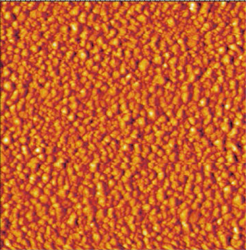
In this article we have synthesized multilayer contact systems Ti/Ag and Ti/Mo/Ag with nanostructured silver films using two vacuum methods, namely the method of electron-beam evaporation and HF magnetron sputtering. Using the data of atomic force microscopy, X-ray diffraction and mass spectroscopy of the secondary neutrals in the paper we have investigated the influence of the application method and of the annealing conditions on the grain formation processes in silver thin films and mass transfer between the metal layers of the contact system. The decrease of surface resistivity of the developed contacts and, respectively, the increase of short-circuit current of the heterojunction silicon solar cells have been determined.References
- JHA, A.R. Solar Cell Technology and Applications. Boca Raton: CRC Press LLC, 2009, 308 p.
- KIM, D.S.; LEE, E.J.; KIM, J.; LEE, S.H. Low-cost contact formation of high-efficiency crystalline silicon solar cells by plating. J. Korean Phys. Soc., 2005, v.46, n.5, p.1208-1212, DOI: http://dx.doi.org/10.3938/jkps.46.1208.
- HOENIG, R.; DUERRSCHNABEL, M.; MIERLO, W.; AABDIN, Z.; BERNHARD, J.; BISKUPEK, J.; EIBL, O.; KAISER, U.; WILDE, J.; CLEMENT, F.; BIRO, D. The nature of screen printed front side silver contacts—results of the project MikroSol. Energy Procedia, 2013, v.43, p.27-36, DOI: http://dx.doi.org/10.1016/j.egypro.2013.11.085.
- VINOD, P.N. Specific contact resistance measurements of the screen-printed Ag thick film contacts in the silicon solar cells by three-point probe methodology and TLM method. J. Mat. Science: Materials in Electronics, 2011, v.22, n.9, p.1248-1257, DOI: http://dx.doi.org/10.1007/s10854-011-0295-z.
- HILALI, M.M.; ROHATGI, A.; TO, B. A review and understanding of screen-printed contacts and selective-emitter formation. Proc. of 14th Workshop on Crystalline Silicon Solar Cells and Modules, NREL, 8–11 Aug. 2004, Winter Park, Colorado. 2004, p.109-116.
- SOLANKI, C.S. Solar Photovoltaics: Fundamentals, Technologies and Applications. Delhi: PHI Learning Private Limited, 2015, 506 p.
- LUQUE, A.; HEGEDUS, S. Handbook of Photovoltaic Science and Engineering. Chichester: John Wiley & Sons Ltd, 2003, 1180 p.
- CHOR, E.F.; ZHANG, D.; GONG, H.; CHONG, W.K.; ONG, S.Y. Electrical characterization, metallurgical investigation, and thermal stability studies of (Pd, Ti, Au)-based ohmic contacts. J. Appl. Phys., 2000, v.87, n.5, p.2437-2444, DOI: http://dx.doi.org/10.1063/1.372198.
- BELYAEV, A.E.; BOLTOVETS, N.S.; KONAKOVA, R.V.; KUDRYK, Y.Y.; SACHENKO, A.V.; SHEREMET, V.N. Temperature dependence of contact resistance of Au–Ti–Pd2Si–n+–Si ohmic contacts. Semicond. Phys. Quantum Electron. Optoelectron., 2010, v.13, n.4, p.436-438, http://www.journal-spqeo.org.ua/n4_2010/v13n4-2010-p436-438.pdf.
- EZAWA, H.; MIYATA, M.; TATSUMI, K. Alloying behaviour of electroplated Ag film with its underlying Pd/Ti film stack for low resistivity interconnect metallization. J. Alloys Compd., 2014, v.587, p.487-492, DOI: http://dx.doi.org/10.1016/j.jallcom.2013.10.182.
- GREEN, MARTIN A. Ag requirements for silicon wafer-based solar cells. Prog. Photovolt.: Res. Appl., 2011, v.19, n.8, p.911-916, DOI: http://dx.doi.org/10.1002/pip.1125.
- KOVAL, V.M.; BOGDAN, O.V.; YAKYMENKO, Y.I. Nanocrystalline silicon multilayer structures for optoelectronics. Proc. of 2nd Int. Conf. on Nanotechnologies and Biomedical Engineering, ICNBME-2013, 18-20 Apr. 2013, Chisinau, Moldova. 2013, p.208-211, http://www.icnbme.sibm.md/files/icnbme_2013_proc/articles/SECTION%20Nanotechnologies%20and%20Nanomaterials/103.pdf.
- KOVAL, V.; BOGDAN, O.; YAKYMENKO, Y. Study of nanocrystalline silicon thin films for application in solar cells. Proc. of 4th Int. Conf. NANOCON, 23-25 Oct. 2012, Brno, Czech Republic. 2012, p.138-143.
- CHE, Q.; YANG, H.; LU, L.; WANG, Y. A new environmental friendly silver front contact paste for crystalline silicon solar cells. J. Alloys Compd., 2013, v.549, p.221-225, DOI: http://dx.doi.org/10.1016/j.jallcom.2012.09.080.
- GREMENOK, V.F.; TIVANOV, M.S.; ZALESSKIY, V.B. Solar Cells Based on Semiconducting Materials. Minsk: BGU, 2007 [in Russian].
- ANDRIYEVSKIY, R.A.; RAGULYA, A.V. Nanostructured Materials. Moscow: Akademiya, 2005 [in Russian].
- DRAGUNOV, V.P.; NEIZVESTNIY, I.G.; GRIDCHIN, V.A. Foundations of Nanoelectronics: Textbook. Moscow: Logos, 2006 [in Russian].
- VORONOV, S.A.; PEREVERZEVA, L.P.; POPLAVKO, Y.M. Material Physics, Part 1. Kyiv: NTUU KPI, 2004 [in Russian].

Downloads
Published
2016-02-20
Issue
Section
Research Articles

