Modelling and simulation of FinFET circuits with predictive technology models
DOI:
https://doi.org/10.3103/S0735272714120048Keywords:
FinFET technology, low power, noise tolerence, short channel effect, leakage powerAbstract
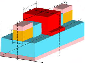
During analysis of complexities of the Metal Oxide Semiconductor Field Effect Transistors (MOSFET) technology to obtain the adequate gate control above the channel, FinFET technology founded on Double or Multiple gate (more than two gates) arrangement is improved technology alternative for auxiliary lessening the size of the MOSFET. In favor of double or dual gate MOSFET (DG MOSFET) the gate control above the channel that formed in between source and drain terminal efficiently. As a result the numerous short channel effects like sub-threshold swing, Drain Induced Barrier Lowering (DIBL-effect), gate leakage current, punch through etc. do not include growing of carrier concentration addicted to the channel. This paper is devoted to specific explanation on the subject of the DG MOSFET composition with its exacting kind termed the same as FinFET technology. FinFET technology has four modes such as shorted-gate (SG) mode, low power (LP) mode, independent-gate (IG) mode and hybrid IG/LP mode and performed the comparative analysis of stand-by leakage (when the circuit is idle), delay, total power consumption and noise of the circuit, using Cadence Virtuoso tool at 45 nm.
References
- JOVANOVIĆ, V.; SULIGOJ, T.; BILJANOVIĆ, P.; NANVER, L.K. FinFET technology for wide-channel devices with ultra-thin silicon body. Proc. of 31st Int. Convention on Information and Communication Technology, Electronics and Microelectronics, MIPRO2008, May 26-30, 2008, Opatija, Croatia, http://ectm.ewi.tudelft.nl/publications_pdf/document1263.pdf.
- KUMAR, V. RAJ; KIRUBARAJ, A. ALFRED. Submicron 70nm CMOS logic design with FINFETs. Int. J. Eng. Sci. Technol., 2010, v.2, n.9, p.4751-4758, http://www.ijest.info/docs/IJEST10-02-09-154.pdf.
- GU, JIE; KEANE, JOHN; SAPATNEKAR, SACHIN; KIM, CHRIS. Width quantization aware FinFET circuit design. Proc. of IEEE Conf. on Custom Integrated Circuits, CICC’06, 10-13 Sept. 2006, San Jose, CA. IEEE, 2006, p.337-340, DOI: http://dx.doi.org/10.1109/CICC.2006.320916.
- CARLSON, A.; GUO, Z.; BALASUBRAMANIAN, S.; PANG, L.T.; LIU, T.-J. KING; NIKOLIC, B. FinFET SRAM with enhanced read/write margins. Proc. of IEEE Int. Conf. SOI, 2-5 Oct. 2006, Niagara Falls, NY. IEEE, 2006, p.105-106, DOI: http://dx.doi.org/10.1109/SOI.2006.284456.
- MUTTREJA, A.; AGARWAL, N.; JHA, N.K. CMOS logic design with independent-gate FinFETs. Proc. of 25th Int. Conf. on Computer Design, ICCD, 7-10 Oct. 2007, Lake Tahoe, CA. IEEE, 2007, p.560-567, DOI: http://dx.doi.org/10.1109/ICCD.2007.4601953.
- LIO, JIA; LUO, ZHIJIONG; YIN, HAIZHOU; ZHU, HUILONG; WANG, HEFEI; YUAN, FENG. Low leakage bulk silicon substrate based SDOI FINFETs. Proc. of 10th IEEE Int. Conf. on Solid-State and Integrated Circuit Technology, ICSICT, 1-4 Nov. 2010, Shanghai. IEEE, 2010, p.1820-1822, DOI: http://dx.doi.org/10.1109/ICSICT.2010.5667687.
- DATTA, ANIMESH; GOEL, ASHISH; CAKICI, RIZA TAMER; MAHMOODI, HAMID; LEKSHMANAN, DHEEPA; ROY, KAUSHIK. Modeling and circuit synthesis for independently controlled double gate FinFET devices. IEEE Trans. CAD Integr. Circuits Syst., Nov. 2007, v.26, n.11, p.1957-1966, DOI: http://dx.doi.org/10.1109/TCAD.2007.896320.
- ROSTAMI, MASOUD; MOHANRAM, KARTIK. Dual-Vth independent-gate FinFETs for low power logic circuits. IEEE Trans. CAD Integr. Circuits Syst., Mar. 2011, v.30, n.3, p.337-339, DOI: http://dx.doi.org/10.1109/TCAD.2010.2097310.
- SHANAVAS, I. HAMEEM; BRINDHA, M.; NALLUSAMY, V. An analogous computation of different techniques for the digital implementation of inverter and NAND logic gates. Int. J. Inf. Eng. Electronic Business, Aug. 2012, v.4, n.4, p.33-38, URL: http://www.mecs-press.org/ijieeb/ijieeb-v4-n4/v4n4-5.html.
- CHIANG, MENG-HSUEH; KIM, KEUNWOO; CHUANG, CHING-TE; TRETZ, C. High-density reduced-stack logic circuit techniques using independent-gate controlled double-gate devices. IEEE Trans. Electron Devices, Sept. 2006, v.53, n.9, p.2370-2377, DOI: http://dx.doi.org/10.1109/TED.2006.881052.
- NARENDAR, V.; R, WANJUL DATTATRAY; RAI, SANJEEV; MISHRA, R.A. Design of high-performance digital logic circuits based on FinFET technology. Int. J. Computer Applications, Mar. 2012, v.41, n.20, p.40-44, DOI: http://dx.doi.org/10.5120/5812-8104.
- DEEPAK, LOURTS A.; DHULIPALLA, LIKHITHA. Design and implementation of 32nm FINFET based 4x4 SRAM cell array using 1-bit 6T SRAM. Proc. of Int. Conf. on Nanoscience, Engineering and Technology, ICONSET, 28-30 Nov. 2011, Chennai. IEEE, 2011, p.177-180, DOI: http://dx.doi.org/10.1109/ICONSET.2011.6167948.
- KIM, N.S.; AUSTIN, T.; BAAUW, D.; MUDGE, T.; FLAUTNER, K.; HU, J.S.; IRWIN, M.J.; KANDEMIR, M.; NARAYANAN, V. Leakage current: Moore’s law meets static power. Computer, Dec. 2003, v.36, n.12, p.68-75, DOI: http://dx.doi.org/10.1109/MC.2003.1250885.
- TAWFIK, SHERIF A.; KURSUN, VOLKAN. Low-power and compact sequential circuits with independent-gate FinFETs. IEEE Trans. Electron Devices, Jan. 2008, v.55, n.1, p.60-70, DOI: http://dx.doi.org/10.1109/TED.2007.911039.
- RAJ, BALWINDER; SAXENA, A.K.; DASGUPTA, S. Nanoscale FinFET based SRAM cell design: Analysis of performance metric, process variation, underlapped FinFET, and temperature effect. IEEE Circuits and Systems Magazine, 2011, v.11, n.3, p.38-50, DOI: http://dx.doi.org/10.1109/MCAS.2011.942068.
- RETDIAN, N.; TAKAGI, S.; FUJII, N. Voltage controlled ring oscillator with wide tuning range and fast voltage swing. Proc. of IEEE Asia-Pacific Conf., ASIC, 2002. IEEE, 2002, p.201-204, DOI: http://dx.doi.org/10.1109/APASIC.2002.1031567.
- LIU, XI; WU, MEILE; JIN, XIAOSHI; CHUAI, RONGYAN; LEE, JUNG-HEE; LEE, JONG-HO. The optimal design of 15 nm gate-length junctionless SOI FinFETs for reducing leakage current. Semicond. Sci. Tech., 2013, v.28, n.10, p.105013, DOI: http://dx.doi.org/10.1088/0268-1242/28/10/105013.


