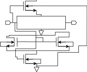
Design and optimization of flash type analog to digital converter using augmented sleep transistors with current mode logic
DOI:
https://doi.org/10.3103/S0735272713100026Keywords:
leakage power, ASTCML logic, Flash type analog to digital converter, ADCAbstract
This paper represents the low leakage & the delay performance optimization of Flash type Analog to Digital converter using Augmented Sleep Transistors with Current Mode Logic (ASTCML) at 45 nm technology. It is realized that the leakage power is reduced 50% approximately in ASTCML logic based analog to digital converter design at 1 V supply voltage. Due to reduced leakage power, the probability of causing thermal runaway is decreased and the design stagnation is increased. Even though the featured analog to digital converter is designed using combination of PMOS and NMOS. The anticipated analog to digital converter is appropriate for high speed and wireless network application. In this paper, different consecutive designs with flash type analog to digital converter are represented.
References
- SETHURAM, R.; ARABI, K.; ABU-RAHMA, M. Leakage power profiling and leakage power reduction using DFT hardware. Proc. of 29th IEEE VLSI Test Symposium (VTS), 1–5 May 2011, Dana Point, CA, USA. Dana Point, 2011, p. 46-51. doi: http://dx.doi.org/10.1109/VTS.2011.5783753">10.1109/VTS.2011.5783753.
- KHOURI, K.S. AND JHA, N.K. Leakage power analysis and reduction during behavioral synthesis. IEEE Trans. Very Large Scale Integration (VLSI) Systems, v.10, n.6, p.876-885, Dec. 2002. doi: http://dx.doi.org/10.1109/TVLSI.2002.808436">10.1109/TVLSI.2002.808436.
- HALTER, J.P. AND NAJM, F.N. A gate-level leakage power reduction method for ultra-low-power CMOS circuits. Proc. of IEEE Custom Integrated Circuits Conf. (CICC), 5–8 May 1997, Santa Clara, CA, USA. Santa Clara, 1997, p. 475-478. doi: http://dx.doi.org/10.1109/CICC.1997.606670">10.1109/CICC.1997.606670.
- TUAN, T. AND LAI, B. Leakage power analysis of a 90nm FPGA. Proc. of IEEE Custom Integrated Circuits Conf. (CICC), 21-24 Sept. 2003, 2003, p. 57-60. doi: http://dx.doi.org/10.1109/CICC.2003.1249359">10.1109/CICC.2003.1249359.
- CHUN, JAE WOONG; CHEN, C.Y.R. A novel leakage power reduction technique for CMOS circuit design. Proc. of SoC Design Conf. (ISOCC), 22-23 Nov. 2010, Seoul, South Korea. Seoul, 2010, p. 119-122. doi: http://dx.doi.org/10.1109/SOCDC.2010.5682957">10.1109/SOCDC.2010.5682957.
- JALAN, A. AND KHOSLA, M. Analysis of leakage power reduction techniques in digital circuits. Proc. of Annual IEEE India Conf. (INDICON), 16–18 Dec. 2011, Hyderabad, India. Hyderabad, 2011, p. 1-4. doi: http://dx.doi.org/10.1109/INDCON.2011.6139374">10.1109/INDCON.2011.6139374.
- YEAP, GARY. Practical Low Power Digital VLSI Design. Kluwer Academic Publishers, 1998.
- LI, LISHA; RAGHAVENDRAN, SRIPRIYA; COMER, DONALD T. CMOS current mode logic gates for high-speed applications. Proc. of 12th NASA Symp. on VLSI Design, 4–5 Oct. 2005, Coeur d’Alene, Idaho, USA. Coeur d’Alene, 2005.
- ALLAM, MOHAMED W. AND ELMASRY, MOHAMED I. Dynamic current mode logic (DyCML): A new low-power high-performance logic style. IEEE J. Solid-State Circuits, v.36, n.3, p.550-558, Mar. 2001. doi: http://dx.doi.org/10.1109/4.910495">10.1109/4.910495.
- RAJANI, H.P. AND KULKARNI, SRIMANNARAYAN. Novel sleep transistor techniques for low leakage power peripheral circuits. Int. J. VLSI design & Commun. Syst., v.3, n.4, 2012. doi: http://dx.doi.org/10.5121/vlsic.2012.3408">10.5121/vlsic.2012.3408.
- SHARMA, VIJAY KUMAR; AND SONI, SURENDER. Comparison among different CMOS inverter for low leakage at different technologies. Int. J. Appl. Eng. Res. Dindigul, v.1, n.2, p.228-233, 2010.
- GHAFARI, P.; ANIS, M.; ELMASRY, M. Impact of technology scaling on leakage reduction techniques. IEEE Northeast Workshop on Circuit and Systems, 5–8 Aug. 2007, Montreal, Que. Montreal, 2007, p.1405-1408. doi: http://dx.doi.org/10.1109/NEWCAS.2007.4488021">10.1109/NEWCAS.2007.4488021.
- ROY, S. AND PAL, A. Impact of runtime leakage reduction techniques on delay and power sensitivity under effective channel length variations. Proc. of IEEE Region 10 Conf. TENCON 2008, 19–21 Nov. 2008, Hyderabad, India. Hyderabad, 2008, p. 1-6. doi: http://dx.doi.org/10.1109/TENCON.2008.4766400">10.1109/TENCON.2008.4766400.
- KHANDELWAL, V. AND SRIVASTAVA, A. Leakage control through fine-grained placement and sizing of sleep transistors. IEEE Trans. CAD Integr. Circuits Syst., v.26, n.7, p.533-536, July 2004. doi: http://dx.doi.org/10.1109/TCAD.2006.888282">10.1109/TCAD.2006.888282.
- RANI, M. JANAKI AND MALARKANN, S. Leakage power reduction and analysis of CMOS sequential circuits. Int. J. VLSI design & Commun. Syst., v.3, n.1, p.13-23, 2012. doi: http://dx.doi.org/10.5121/vlsic.2012.3102">10.5121/vlsic.2012.3102.
- AUGSBURGER, S. AND NIGOLIC, B. Combining dual-supply, dual-threshold and transistor sizing for power reduction. Proc. of IEEE Int. Conf. “Computer Design: VLSI in Computers and Processors,” 2002, p. 316-321. doi: http://dx.doi.org/10.1109/ICCD.2002.1106788">10.1109/ICCD.2002.1106788.
- WASTE, NEIL H.E. AND ESHRAGHIAN, K. Principles of CMOS Design: A System Perspective, 2nd ed. Pearson Publication, Inc. and Dorling Kindersley Publishing, Inc., 2000.
- KUMAR, DEEPAK; KUMAR, PANKAJ; PATTANAIK, MANISHA. Performance analysis of dynamic threshold MOS (DTMOS) 4-input multiplexer switch for low power and high speed FPGA design. Proc. 23rd Symp. “Integrated Circuits and System Design,” SBCCI’10, Sept. 2010, 2010, p.2-7. doi: http://dx.doi.org/10.1145/1854153.1854156">10.1145/1854153.1854156.
- SYLVESTER, D. AND KAUL, H. Future performance challenges in nanometer design. Proc. of DAC 2001, June 18–22, 2001, Las Vegas, Nevada, USA. Las Vegas, 2001, p.3-8.
- KUMAR, PRADEEP AND KOLHE, AMIT. Design & implementation of low power 3-bit flash ADC in 0.18mm CMOS. Int. J. Soft Comput. Eng., v.1, n.5, p.71-74, 2011, http://www.ijsce.org/attachments/File/Vol-1_Issue-5/ E0150081511.pdf "> http://www.ijsce.org/attachments/File/Vol-1_Issue-5/ E0150081511.pdf .
- SHEHATA, K.A.; RAGAI, H.F.; HUSIEN, H. Design and implementation of a high speed low power 4-bit Flash ADC. Proc. of IEEE Int. Conf. “Design & Technology of Integrated Systems in Nanoscale Era” (DTIS), 2–5 Sept. 2007, Rabat, Morocco. Rabat, 2007, p.200-203. doi: http://dx.doi.org/10.1109/DTIS.2007.4449519">10.1109/DTIS.2007.4449519.
- AL-IBRAHIM, M.M.; BATAINEH, S.; IRSHID, M. A new fast analog-to-digital counting converter. Proc. of Third IEEE Int. Conf. “Electronics, Circuits & Systems,” ICECS’96, 13–16 Oct 1996, Rhodes, Greece. Rhodes, 1996, v.2, p.912-915. doi: http://dx.doi.org/10.1109/ICECS.1996.584533">10.1109/ICECS.1996.584533.
- VEERAMACHANEN, S.; KUMAR, A.M.; TUMMALA, V.; SRINIVAS, M.B. Design of a low power, variable-resolution flash ADC. Proc. of 22nd Int. Conf. VLSI Design, 5–9 Jan. 2009, New Delhi, India. New Delhi, 2009, p.117-122. doi: http://dx.doi.org/10.1109/VLSI.Design.2009.62">10.1109/VLSI.Design.2009.62.
- SHARMA, VIJAY KUMAR AND SONI, SURENDER. Comparison among different CMOS inverter for low leakage at different technologies. Int. J. Appl. Eng. Res. Dindigul, v.1, n.2, 2010, http://www.ipublishing.co.in/jarvol1no12010/EIJAER1021.pdf "> http://www.ipublishing.co.in/jarvol1no12010/EIJAER1021.pdf .
- SINGH, AJAY KUMAR. Digital VLSI Design. PHI Publication, 2011.
- YOO, JINCHEOL; CHOI, KYUSUN; TANGEL, ALI. A 1-GSPS CMOS flash A/D converter for system-on-chip applications. IEEE Computer Society Workshop on VLSI, WVLSI’01, 2001, p.135-139.
- RICHARDS, T.C. Dynamic testing of A/D converters using the coherence function. IEEE Trans. Instrum. Meas., v.55, n.6, p.2265-2274, Dec. 2006. doi: http://dx.doi.org/10.1109/TIM.2006.884127">10.1109/TIM.2006.884127.


