Transient model for modern microelectronic devices applicable to EKV PMOS model
DOI:
https://doi.org/10.3103/S0735272721020023Keywords:
spline collocation method, quasi static approach, symmetrical telescopic modification, normalized channel charge densities, EKV PMOS modelAbstract
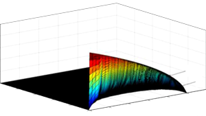
Massive advances in microelectronic manufacturing technology with an exponential growth of their complexity and speed are needed to ensure a continuous development of novel techniques, structures, devices, circuits and systems. This paper is intended for the introduction of a new PMOS transient model for modern microelectronic devices that provides a fast transient response. Such suggested model expresses the transient terminal currents as polynomial functions of the normalized channel charge densities at the channel bounds with the assistance of a modified version of the cubic spline collocation methodology in symmetrical telescopic fashion. Additionally, the optimum number of segments, which is suitable for the new version of the cubic spline collocation algorithm, is investigated. Moreover, the normalized channel charge density at collocation points is modeled in terms of its values at the channel bounds through the quasi-static approach. Furthermore, by means of introducing an inverse function for the normalized overdrive channel voltage, the transient terminal currents are formulated as a function of the terminal voltages. In comparison with usual cubic spline collocation structure, the novel model has much better accuracy in its application to EKV structure. The developed model has been applied to the standard 0.15 mm technology and validated by MATLAB R2014a. The obtained results demonstrate that it gives a very high degree of relative accuracy, on average of 99%, for the total time and exhibits absolute error of less than 5% of the maximum value, in its worst case.
References
S.-Y. Oh, D. E. Ward, R. W. Dutton, “Transient analysis of MOS transistors,” IEEE J. Solid-State Circuits, vol. 15, no. 4, pp. 636–643, 1980, doi: https://doi.org/10.1109/JSSC.1980.1051448.
A. S. Roy, J. M. Vasi, M. B. Patil, “A new approach to model nonquasi-static (NQS) effects for mosfets-part I: large-signal analysis,” IEEE Trans. Electron Devices, vol. 50, no. 12, pp. 2393–2400, 2003, doi: https://doi.org/10.1109/TED.2003.819053.
C. C. Enz, E. A. Vittoz, Charge-Based MOS Transistor Modeling. Chichester, UK: John Wiley & Sons, Ltd, 2006, doi: https://doi.org/10.1002/0470855460.
A. J. Scholten, L. F. Tiemeijer, P. W. H. De Vreede, D. B. M. Klaassen, “A large signal non-quasi-static MOS model for RF circuit simulation,” in International Electron Devices Meeting 1999. Technical Digest (Cat. No.99CH36318), 1999, pp. 163–166, doi: https://doi.org/10.1109/IEDM.1999.823870.
H. Wang, T.-L. Chen, G. Gildenblat, “Quasi-static and nonquasi-static compact mosfet models based on symmetric linearization of the bulk and inversion charges,” IEEE Trans. Electron Devices, vol. 50, no. 11, pp. 2262–2272, 2003, doi: https://doi.org/10.1109/TED.2003.818596.
M. B. El Mashade, A. A. M. Afifi, T. Dabbous, “A new design methodology for enhancing the transient loading of low drop-out regulators (LDRs),” Int. J. Electron. Telecommun., vol. 65, no. 2, pp. 325–333, 2019, uri: http://ijet.pl/index.php/ijet/article/view/10.24425-ijet.2019.126317.
CADANCE, Virtuoso UltraSim Simulator User Guide, Product Version 7.2, May 2010. CADANCE, 2010, uri: http://picture.iczhiku.com/resource/eetop/WYiGePwqkEhquBcc.pdf.
R. J. Milliken, J. Silva-Martinez, E. Sanchez-Sinencio, “Full on-chip CMOS low-dropout voltage regulator,” IEEE Trans. Circuits Syst. I Regul. Pap., vol. 54, no. 9, pp. 1879–1890, 2007, doi: https://doi.org/10.1109/TCSI.2007.902615.
C. Hu, C. Enz, “EKV MOSFET Model.” https://www.epfl.ch/labs/iclab/ekv/.
A. A. Afifi, M. B. El Mashade, T. E. Dabbous, “Cubic sp-line collocation enhancement for modeling of MOS transient,” Int. J. Recent Technol. Eng., vol. 8, no. 1, pp. 920–926, 2019, uri: https://www.ijrte.org/wp-content/uploads/papers/v8i1/F2340037619.pdf.
S.Y. Oh, D. Ward, and R. Dutton, Transient Analysis of MOS Transistors, IEEE Journal of Solid-State Circuits, SC-15, pp. 636-643, 1980.
A. S. Roy, J. M. Vasi, and M. B. Patil, “A new approach to model nonquasi-static (NQS) effects for MOSFETs—Part I: Large-signal analysis, ”IEEE Trans. Electron Devices, vol. 50, no. 12, pp. 2393–2400,Dec. 2003.
Christian C. Enz & Eric A. Vittoz, " Charge-based MOS Transistor Modeling", John Wiley & Sons Ltd, 2006.
A. J. Scholten, L. F. Tiemeijer, P.W. H. de Vreede, and D. B.M. Klaassen,“A large signal non-quasi-static MOS model for RF circuit simulation,” in IEDM Tech. Dig., 1999, pp. 163–166.
H. Wang, T.-L. Chen, and G. Gildenblat, “Quasi-static and nonquasistatic compact MOSFET models based on symmetric linearization of the bulk and inversion charges,” IEEE Trans. Electron Devices, vol. 50, no. 11, pp. 2262–2272, Nov. 2003.
Ahmed Abdel_Monem, Mohamed B. El_Mashade, and T. E. Dabbous, “A New Design Methodology For Enhancing the Transient Loading Of Low Drop-out Regulators (LDRs)”, INTL Journal of Electronics and Telecommunications, 2019, Vol. 65, No.2, pp. 325-333, April, 2019. DOI: 10.24425/ijet.2019.126318
VIRTUOSO Simulator Circuit Components and Devices Models Manual, CADANCE, Product Version 7.2, May 2010.
Robert J. Milliken, Jose Silva-Martínez, and Edgar Sánchez-Sinencio, “Full On-Chip CMOS Low-Dropout Voltage Regulator”, IEEE Transaction on Circuits and Systems, Vol. 54, No. 9, SEPTEMBER 2007, pp. 1879-1890.
http://ekv.epfl.ch/page-44591-en.html.
Ahmed A. Afifi, Mohamed B. El_Mashade, T. E. Dabbous, “Cubic Sp-line Collocation Enhancement for Modeling of MOS Transient”, International Journal of Recent Technology and Engineering (IJRTE), Vol. 8, Issue-1, May 2019, pp. 920-926.