Decrease of surface recombination in single-crystalline silicon by means of pulse laser film deposition with silicon quantum points
DOI:
https://doi.org/10.3103/S0735272722030037Abstract
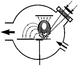
In this paper it is proposed a method of suppress of surface recombination in c-Si by means of modification of its surface with nanoparticles. Silicon nanocomposites containing quantum-dimensional particles of Si in SiO2 matrix characterized with increased width of forbidden states in case of its deposition at c-Si substrate shape a heterojunction nc-Si/c-Si whose potentional barrier promotes the surface charge carriers lifetime increase. The experimental results are represented. The method is tested in industrial conditions using technology silicon slices. It is proved the possibility of decrease of surface recombination in single-crystalline silicon by means of its surface passivation in case of pulse laser deposition of films with silicon quantum points.
References
S. Jariwala et al., “Reducing surface recombination velocity of methylammonium-free mixed-cation mixed-halide perovskites via surface passivation,” Chem. Mater., vol. 33, no. 13, pp. 5035–5044, 2021, doi: https://doi.org/10.1021/acs.chemmater.1c00848.
K. Zhang, X. Li, A. C. Walhof, Y. Liu, F. Toor, J. P. Prineas, “Long interior carrier lifetime in selective-area InAs nanowires on silicon,” Opt. Mater. Express, vol. 10, no. 10, p. 2470, 2020, doi: https://doi.org/10.1364/OME.403531.
H. Wu et al., “A correlative study of film lifetime, hydrogen content, and surface passivation quality of amorphous silicon films on silicon wafers,” IEEE J. Photovoltaics, vol. 10, no. 5, pp. 1307–1312, 2020, doi: https://doi.org/10.1109/JPHOTOV.2020.3009146.
M. Nagesh, R. Suresh, R. Jayapal, K. N. Subramanya, “Surface passivation studies of n-type crystalline silicon for HIT solar cells,” Trans. Electr. Electron. Mater., vol. 23, no. 1, pp. 45–51, 2022, doi: https://doi.org/10.1007/s42341-021-00316-1.
D. Muchahary, S. Maity, S. K. Metya, “Modelling and analysis of temperature‐dependent carrier lifetime and surface recombination velocity of Si-ZnO heterojunction thin film solar cell,” Micro Nano Lett., vol. 14, no. 4, pp. 399–403, 2019, doi: https://doi.org/10.1049/mnl.2018.5147.
J. Cui, N. Grant, A. Lennon, “Effective surface passivation of p-type crystalline silicon with silicon oxides formed by light-induced anodisation,” Appl. Surf. Sci., vol. 323, pp. 40–44, 2014, doi: https://doi.org/10.1016/j.apsusc.2014.08.028.
J. N. Heyman, A. Sahu, N. E. Coates, B. Ehmann, J. J. Urban, “Carrier lifetime enhancement in a tellurium nanowire/PEDOT:PSS nanocomposite by sulfur passivation,” MRS Proc., vol. 1742, pp. mrsf14-1742-bb04-02, 2015, doi: https://doi.org/10.1557/opl.2015.157.
D. J. Michalak, F. Gstrein, N. S. Lewis, “The role of band bending in affecting the surface recombination velocities for Si(111) in contact with aqueous acidic electrolytes,” J. Phys. Chem. C, vol. 112, no. 15, pp. 5911–5921, 2008, doi: https://doi.org/10.1021/jp075354s.
R. S. Bonilla, C. Reichel, M. Hermle, S. Senkader, P. Wilshaw, “Controlled field effect surface passivation of crystalline n-type silicon and its application to back-contact silicon solar cells,” in 2014 IEEE 40th Photovoltaic Specialist Conference (PVSC), 2014, pp. 0571–0576, doi: https://doi.org/10.1109/PVSC.2014.6924985.
J. Linnros, “Carrier lifetime measurements using free carrier absorption transients. I. Principle and injection dependence,” J. Appl. Phys., vol. 84, no. 1, pp. 275–283, 1998, doi: https://doi.org/10.1063/1.368024.
V. Palermo, D. Jones, “Self-organised growth of silicon structures on silicon during oxide desorption,” Mater. Sci. Eng. B, vol. 88, no. 2–3, pp. 220–224, 2002, doi: https://doi.org/10.1016/S0921-5107(01)00867-4.
H. Yamada, “Microscopic composition difference related to oxidizing humidity near the ultrathin silicon oxide–Si(100) interface,” J. Vac. Sci. Technol. A Vacuum, Surfaces, Film., vol. 19, no. 2, pp. 627–632, 2001, doi: https://doi.org/10.1116/1.1351065.
K. Fujita, H. Watanabe, M. Ichikawa, “Scanning tunneling microscopy study on void formation by thermal decomposition of thin oxide layers on stepped Si surfaces,” J. Appl. Phys., vol. 83, no. 8, pp. 4091–4095, 1998, doi: https://doi.org/10.1063/1.367162.
G. W. Rubloff, “Defect microchemistry in SiO_2/Si structures,” J. Vac. Sci. Technol. A Vacuum, Surfaces, Film., vol. 8, no. 3, pp. 1857–1863, 1990, doi: https://doi.org/10.1116/1.576816.
I. Martı́n et al., “Improvement of crystalline silicon surface passivation by hydrogen plasma treatment,” Appl. Phys. Lett., vol. 84, no. 9, pp. 1474–1476, 2004, doi: https://doi.org/10.1063/1.1647702.
T. Matsushita et al., “Highly reliable high-voltage transistors by use of the SIPOS process,” IEEE Trans. Electron Devices, vol. 23, no. 8, pp. 826–830, 1976, doi: https://doi.org/10.1109/T-ED.1976.18494.
T. A. Kolbasov, S. V. Volkov, V. S. Vorobets, I. A. Rusetskiy, “Photoelectrochemical processes on GaAs and InP modified by nanosized CdS particles,” Nanosistemy, Nanomater. Nanotekhnologii, vol. 2, no. 1, pp. 169–177, 2004.
R. Ciach et al., “Silicon based multilayer structures prepared by reactive pulsed laser deposition,” Thin Solid Film., vol. 318, no. 1–2, pp. 154–157, 1998, doi: https://doi.org/10.1016/S0040-6090(97)01156-5.
L. Patrone, D. Nelson, V. I. Safarov, M. Sentis, W. Marine, S. Giorgio, “Photoluminescence of silicon nanoclusters with reduced size dispersion produced by laser ablation,” J. Appl. Phys., vol. 87, no. 8, pp. 3829–3837, 2000, doi: https://doi.org/10.1063/1.372421.
E. G. Gule, E. B. Kaganovich, I. M. Kizyak, E. G. Manoilov, S. V. Svechnikov, “Edge photoluminescence of single-crystal silicon at room temperature,” Semiconductors, vol. 39, no. 4, p. 406, 2005, doi: https://doi.org/10.1134/1.1900253.
E. B. Kaganovich, S. I. Kirillova, E. G. Manoilov, V. E. Primachenko, S. V. Svechnikov, “Interface electronic properties of eterojunctions based on nanocrystalline silicon,” Semicond. Physics, Quantum Electron. Optoelectron., vol. 2, no. 2, pp. 11–14, 1999, uri: http://journal-spqeo.org.ua/n2_99/abstr011-014.htm.
E. B. Kaganovich et al., “Photoluminescent films of nanocrystalline silicon doped with metals,” Semicond. Physics, Quantum Electron. Optoelectron., vol. 5, no. 2, pp. 125–132, 2002, uri: http://journal-spqeo.org.ua/n2_2002/abstr125-132.htm.
É. B. Kaganovich et al., “Photoluminescent and electronic properties of nanocrystalline silicon doped with gold,” Semiconductors, vol. 36, no. 9, pp. 1027–1032, 2002, doi: https://doi.org/10.1134/1.1507286.
E. B. Kaganovich, V. K. Maliutenko, E. G. Gule, S. V. Chyrchyk, E. G. Manoilov, “Modification of silicon surface recombination and edge photoluminescence of silicon,” in VI Mezdunarodnyy Ukrainsko-Russkiy Seminar “Nanofizika I Nanoelektronika,” 2005, pp. 101–102.
S. V. Chyrchyk, V. K. Malyutenko, E. G. Gule, E. B. Kaganovich, “Improvement of monocrystalline silicon surface passivation by silicon nanostructure deposition,” in 2nd International Conference on Physics of Laser Crystals, 2005, uri: http://icplc2005.narod.ru/s2005.html.
S. V. Chyrchyk, “Express method of finding recombination parameters in technological silicon plates,” Radioelectron. Commun. Syst., vol. 55, no. 3, pp. 136–139, 2012, doi: https://doi.org/10.3103/S0735272712030053.
S. V. Chyrchyk, “Investigation of recombination parameters of nonequilibrium charge carriers in Si technological plates by thermal imaging method,” Radioelectron. Commun. Syst., vol. 63, no. 9, pp. 488–496, 2020, doi: https://doi.org/10.3103/S0735272720090034.