Analysis and design of low power SRAM cell using independent gate FinFET
DOI:
https://doi.org/10.3103/S0735272713090021Keywords:
FinFET, SRAM, MOSFETAbstract
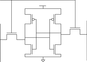
Scaling of bulk MOSFET faces great challenges in nanoscale integration technology by producing short channel effect which leads to increased leakage. FinFET has become the most promising substitute to bulk CMOS technology because of reducing short channel effect. Dual-gate FinFET can be designed either by shorting gates on either side for better performance or both gates can be controlled independently to reduce the leakage and hence power consumption. A six transistor SRAM cell based on independent-gate FinFET technology is described in this paper for simultaneously reducing the active and standby mode power consumption. A work is focused on the independent gate FinFET technology as this mode provides less power consumption, less area consumption and low delay as compared to other modes. Leakage current and power consumption in independent gate FinFET is compared with tied gate or shorted gate FinFET SRAM cell. Moreover, delay has been estimated in presented SRAM cells. Further, leakage reduction technique is applied to independent gate FinFET 6T SRAM cell.
References
- FRANK, D.J.; DENNARD, R.H.; NOWAK, E.; SOLOMON, P.M.; TAUR, YUAN; WONG, HEN-SUM PHILIP. Device scaling limits of Si MOSFETs and their application dependencies. Proc. IEEE, v.89, n.3, p.259-288, Mar. 2001. doi: http://dx.doi.org/10.1109/5.915374">10.1109/5.915374.
- KURSUN, V. AND FRIEDMAN, E.G. Multi-Voltage CMOS Circuit Design. Hoboken, NJ: Wiley, 2006. 242 p.
- FRIED, D.M. The Design, Fabrication and Characterization of Independent-Gate Finfets. Cornell University, 2004. 184 p.
- ROSTAMI, M. AND MOHANRAM, K. Novel dual-Vth independent-gate FinFET circuits. Proc. of 15th IEEE Design Automation Conf. (ASP-DAC), 18–21 Jan. 2010. Asia and South Pasific, 2010, p.867-872. doi: http://dx.doi.org/10.1109/ASPDAC.2010.5419680">10.1109/ASPDAC.2010.5419680.
- CHIN, E.; DUNGA, M.; NIKOLIC, B. Design trade-offs of a 6T FinFET SRAM cell in the presence of variations. IEEE. Symp. VLSI Circuits, 2006, p.445-449.
- TAWFIK, S.A. AND KURSUN, Volkan. Portfolio of FinFET memories: Innovative techniques for an emerging technology. Proc. of IEEE Int. SoC Design Conf., ISOCC’08, 24–25 Nov. 2008. Busan, 2008, v.1, p.I-101–I-104. doi: http://dx.doi.org/10.1109/SOCDC.2008.4815583">10.1109/SOCDC.2008.4815583.
- TAWFIK, SHERIF A. AND KURSUN, V. Low power and stable FinFET SRAM with static independent gate bias for enhanced integration density. Proc. of 14th IEEE Int. Conf. “Electronics, Circuits and Systems,” ICECS 2007, 11–14 Dec. 2007. Marrakech, 2007, p.443-446. doi: http://dx.doi.org/10.1109/ICECS.2007.4511025">10.1109/ICECS.2007.4511025.
- RAJ, B.; SAXENA, A.K.; DASGUPTA, S. Nanoscale FinFET based SRAM cell design: Analysis of performance metric, process variation, underlapped FinFET and temperature effect. IEEE Circuits and Systems Magazine, v.11, n.3, p.38-50, 2001. doi: http://dx.doi.org/10.1109/MCAS.2011.942068">10.1109/MCAS.2011.942068.
- NIRMAL; KUMAR, V.; JABARAJ, S. Nand gate using FinFET for nanoscale technology. Int. J. Eng. Sci. Technol., v.2, n.5, p.1351-1358, May 2010, http://www.ijest.info/docs/IJEST10-02-05-10.pdf"> http://www.ijest.info/docs/IJEST10-02-05-10.pdf.
- SIKARWAR, V.; KHANDELWAL, S.; AKASHE, S. Optimization of leakage current in SRAM cell using shorted gate DG FinFET. Proc. of 3rd IEEE Int. Conf. “Advanced Computing and Communication Technologies,” (ACCT), 6–7 Apr. 2013. Rohtak, 2013, p.166-170. doi: http://dx.doi.org/10.1109/ACCT.2013.41">10.1109/ACCT.2013.41.
- AKASHE, S.; SINHA, D.K.; SHARMA, S. A low-leakage current power 45-nm CMOS SRAM. Indian J. Sci. Technol., v.4, n.4, p.440, 2011, http://www.indjst.org/index.php/indjst/article/view/30019"> http://www.indjst.org/index.php/indjst/article/view/30019.
- RASOULI, S.H.; DADGOUR, H.F.; ENDO, K.; KOIKE, H.; BANERJEE, K. Design optimization of FinFET domino logic considering the width quantization property. IEEE Trans. Electron Devices, v.57, n.11, p.2934-2943, Nov. 2010. doi: http://dx.doi.org/10.1109/TED.2010.2076374">10.1109/TED.2010.2076374.
- KOH, SHAO-MING; SAMUDRA, G.S.; YEO, YEE-CHIA. Contact technology for strained nFinFETs with silicon-carbon source/drain stressors featuring sulfur implant and segregation. IEEE Trans. Electron Devices, v.59, n.4, p.1046-1055, Apr. 2012. doi: http://dx.doi.org/10.1109/TED.2012.2185799">10.1109/TED.2012.2185799.